Training Course on Semiconductor Device Physics and Fabrication

Course Title: Training Course on Semiconductor Device Physics and Fabrication
Executive Summary
This intensive two-week course provides a comprehensive understanding of semiconductor device physics and fabrication techniques. Participants will explore the fundamental principles governing semiconductor behavior, delve into the intricacies of device design, and gain hands-on experience with fabrication processes. The course covers a range of topics, including crystal growth, doping, etching, deposition, and characterization. Emphasis is placed on modern fabrication methods and their impact on device performance. Through lectures, simulations, and laboratory sessions, participants will develop the skills necessary to analyze, design, and fabricate semiconductor devices. This course is ideal for engineers, scientists, and researchers seeking to enhance their knowledge and expertise in the field of semiconductor technology, enabling them to contribute to advancements in microelectronics and nanotechnology.
Introduction
Semiconductor devices are the building blocks of modern electronics, and a thorough understanding of their physics and fabrication is crucial for engineers and scientists working in this field. This course aims to provide participants with a comprehensive overview of semiconductor device physics, covering the fundamental principles that govern the behavior of these devices. Participants will learn about the properties of semiconductor materials, the formation of p-n junctions, the operation of transistors, and the principles of device design. In addition, the course will provide a detailed introduction to semiconductor fabrication techniques, covering topics such as crystal growth, doping, etching, deposition, and lithography. Participants will gain hands-on experience with these techniques through laboratory sessions and simulations. By the end of the course, participants will have a solid foundation in semiconductor device physics and fabrication, enabling them to contribute to the development of advanced electronic devices.
Course Outcomes
- Understand the fundamental principles of semiconductor device physics.
- Analyze the behavior of various semiconductor devices.
- Design and simulate semiconductor devices using industry-standard software.
- Gain practical experience in semiconductor fabrication techniques.
- Characterize the electrical and optical properties of semiconductor devices.
- Apply knowledge of semiconductor technology to real-world applications.
- Contribute to the development of advanced electronic devices and circuits.
Training Methodologies
- Interactive lectures and discussions.
- Hands-on laboratory sessions.
- Computer simulations using industry-standard software.
- Case study analysis of real-world semiconductor devices.
- Group projects and presentations.
- Guest lectures from industry experts.
- Site visits to semiconductor fabrication facilities.
Benefits to Participants
- Enhanced knowledge of semiconductor device physics and fabrication.
- Improved skills in device design and simulation.
- Practical experience in semiconductor fabrication techniques.
- Increased understanding of the latest trends in semiconductor technology.
- Expanded professional network through interaction with peers and industry experts.
- Career advancement opportunities in the semiconductor industry.
- Certification recognizing proficiency in semiconductor device physics and fabrication.
Benefits to Sending Organization
- Improved employee skills and knowledge in semiconductor technology.
- Increased ability to develop and manufacture advanced electronic devices.
- Enhanced innovation and competitiveness in the marketplace.
- Reduced reliance on external consultants and contractors.
- Improved efficiency and productivity in research and development.
- Attraction and retention of top talent in the semiconductor field.
- Enhanced reputation as a leader in semiconductor technology.
Target Participants
- Electrical Engineers
- Electronics Engineers
- Materials Scientists
- Physicists
- Chemical Engineers
- Process Engineers
- Research Scientists
Week 1: Semiconductor Physics and Device Fundamentals
Module 1: Semiconductor Materials and Properties
- Crystal structure of semiconductors (Si, Ge, GaAs).
- Energy bands and bandgap.
- Intrinsic and extrinsic semiconductors.
- Carrier concentration and mobility.
- Doping and its effects on semiconductor properties.
- Temperature dependence of carrier concentration.
- Compound Semiconductors and their advantages
Module 2: P-N Junctions
- Formation of p-n junctions.
- Depletion region and built-in potential.
- Forward and reverse bias characteristics.
- Diode equation.
- Junction capacitance.
- Breakdown mechanisms.
- Applications of p-n junctions (rectifiers, diodes).
Module 3: Bipolar Junction Transistors (BJTs)
- Structure and operation of BJTs (NPN and PNP).
- Current-voltage characteristics.
- Common-emitter, common-base, and common-collector configurations.
- Transistor parameters (gain, saturation voltage, etc.).
- Biasing techniques.
- BJT amplifiers.
- Switching Characteristics of BJTs
Module 4: Metal-Oxide-Semiconductor Field-Effect Transistors (MOSFETs)
- Structure and operation of MOSFETs (NMOS and PMOS).
- Enhancement and depletion mode MOSFETs.
- Threshold voltage.
- Current-voltage characteristics.
- MOSFET parameters (transconductance, output resistance, etc.).
- CMOS logic circuits.
- Scaling and short-channel effects.
Module 5: Device Modeling and Simulation
- Introduction to device modeling.
- Compact models (SPICE models).
- Numerical simulation tools (TCAD).
- Simulation of p-n junctions, BJTs, and MOSFETs.
- Parameter extraction.
- Model calibration and validation.
- Using simulation to optimize device performance.
Week 2: Semiconductor Fabrication Techniques and Advanced Devices
Module 6: Crystal Growth and Wafer Preparation
- Crystal growth techniques (Czochralski, Float Zone).
- Wafer slicing, lapping, and polishing.
- Wafer cleaning and surface preparation.
- Epitaxial growth.
- Silicon-on-insulator (SOI) technology.
- Wafer characterization techniques.
- Advanced Substrates for device fabrication
Module 7: Doping and Diffusion
- Diffusion theory.
- Ion implantation.
- Rapid thermal annealing (RTA).
- Dopant activation and redistribution.
- Diffusion sources and methods.
- Junction formation techniques.
- Process control and optimization.
Module 8: Etching and Deposition
- Wet etching.
- Dry etching (plasma etching, reactive ion etching).
- Chemical vapor deposition (CVD).
- Physical vapor deposition (PVD).
- Atomic layer deposition (ALD).
- Thin film characterization.
- Selective Etching techniques.
Module 9: Lithography and Patterning
- Optical lithography.
- Deep ultraviolet (DUV) lithography.
- Electron beam lithography.
- X-ray lithography.
- Mask design and fabrication.
- Resist processing.
- Resolution enhancement techniques.
Module 10: Advanced Semiconductor Devices and Technologies
- FinFETs and other advanced transistor structures.
- Memory devices (DRAM, SRAM, Flash).
- Solar cells.
- Sensors and MEMS devices.
- Emerging materials (GaN, SiC).
- 3D integration.
- Nanotechnology and nanoelectronics.
Action Plan for Implementation
- Conduct a gap analysis of current semiconductor knowledge and skills.
- Develop a training plan based on the course outcomes and organizational needs.
- Implement the training plan, incorporating the methodologies learned in the course.
- Monitor the effectiveness of the training through pre- and post-training assessments.
- Provide ongoing support and mentorship to participants.
- Encourage participants to apply their new knowledge and skills to real-world projects.
- Evaluate the impact of the training on organizational performance and make adjustments as needed.
Course Features
- Lecture 0
- Quiz 0
- Skill level All levels
- Students 0
- Certificate No
- Assessments Self
You May Like

Advanced Population Ecology and Demographics
Course Title: Advanced Population Ecology and Demographics Executive Summary This intensive two-week course on Advanced Population Ecology and Demographics equips participants with advanced quantitative and...

Applied Conservation Genetics for Species Management
Course Title: Applied Conservation Genetics for Species Management Executive Summary This two-week intensive course on Applied Conservation Genetics for Species Management bridges the gap between...
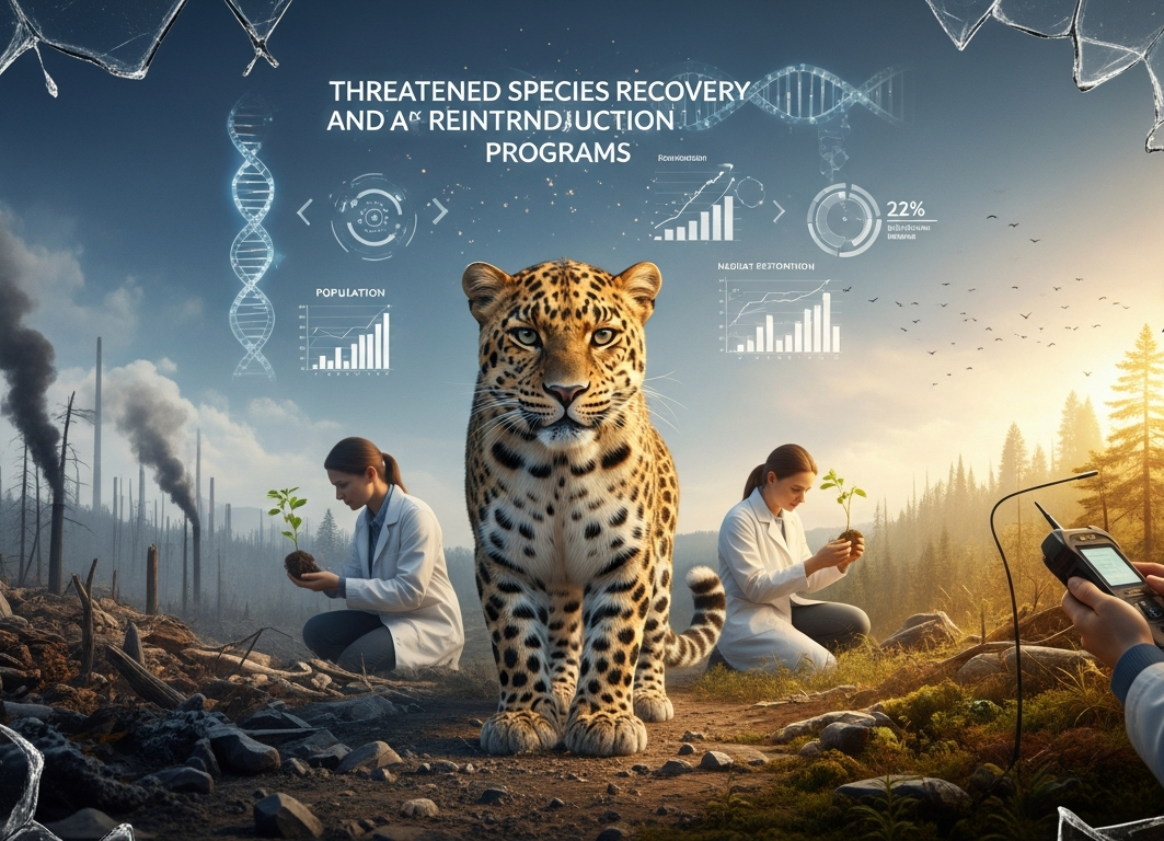
Threatened Species Recovery and Reintroduction Programs
Course Title: Threatened Species Recovery and Reintroduction Programs Executive Summary This intensive two-week course provides a comprehensive framework for designing, implementing, and managing recovery plans...

Landscape Ecology and Connectivity Science Training Course
Course Title: Landscape Ecology and Connectivity Science Training Course Executive Summary This intensive two-week executive course on Landscape Ecology and Connectivity Science is designed to...
Biodiversity Hotspot Conservation and Management
Course Title: Biodiversity Hotspot Conservation and Management Executive Summary This intensive two-week course on Biodiversity Hotspot Conservation and Management equips participants with the knowledge and...